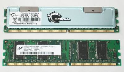
DDR SDRAM

The memory chips are available DDR SDRAM in TSOP and (mastered later) packages such as BGA (FBGA), produced by 0.13-and 0.09-micron process technology
Power supply circuits: 2.6 V + / - 0.1
Power consumption: 527 mW
Input-output interface: SSTL_2
The memory bus is 64 bits, that is, on the bus in one clock cycle simultaneously transferred 8 bytes. As a result, we obtain the following formula to calculate maximum throughput for a given type of memory: the memory bus clock x 2 (data twice per clock cycle) x 8 (number of bytes transmitted per clock cycle). For example, to ensure the transfer of data twice per clock cycle, a special architecture «2n Prefetch». The internal data bus width is twice the outside. When transferring data is first passed to the first half of the data bus in front of the clock signal, and then the second half of the data bus in a recession.
In addition to twice the data transfer, DDR SDRAM has several other fundamental differences from simple memory SDRAM. In general, they are technological. For example, the signal was added QDS, which is located on the PCB along the lines of data. On it synchronizes the data transfer. If you are using two memory modules, the data from them come to the memory controller with a slight difference due to different distances. The problem arises in the choice of timing for reading and the use of QDS is successfully solved.
JEDEC sets the standards for speeds of DDR SDRAM, divided into two parts: one for the memory chips, and the second memory module, which, in fact, placed the memory chips.
